Laying the VLSI Foundation
Introduction to VLSI & the Chip Design Lifecycle
Before we write a single line of code, let's zoom out and look at the big picture. What is this "chip" we're trying to design, and what is the industrial process to create one?
An Integrated Circuit (IC), or a chip, is a miniature electronic circuit built on a small piece of semiconductor material, usually silicon. VLSI (Very Large Scale Integration) is the process of creating these ICs by combining millions or even billions of microscopic transistors into a single chip. Every modern electronic device, from your smartphone to a supercomputer, is powered by VLSI chips.
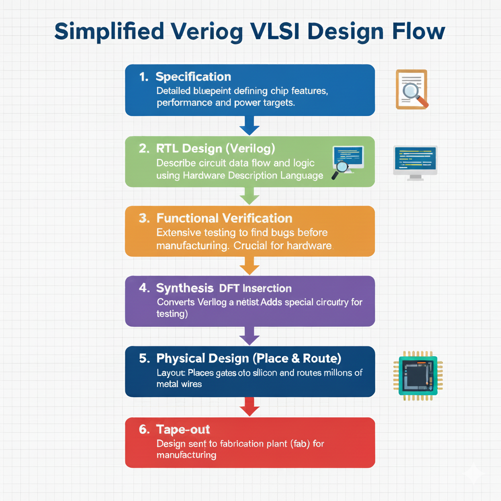
Writing Verilog code is just one step in a long and complex industrial process called the VLSI Design Flow. Understanding this flow is crucial because it gives context to why we write code in a specific way.

The major stages are:
Specification: This is the starting point. It's a document (like a detailed blueprint) that defines everything the chip is supposed to do, including its features, performance targets, and power consumption.
RTL Design: This is where we come in. RTL (Register Transfer Level) is a way of describing a digital circuit by defining how data moves between registers (storage elements like flip-flops) and the logical operations performed on that data. We write RTL code using a Hardware Description Language (HDL) like Verilog.
Functional Verification: This is one of the most time-consuming phases. A separate team of engineers writes an enormous amount of code to test our RTL design, trying every possible scenario to find bugs before the chip is made. You can't patch hardware!
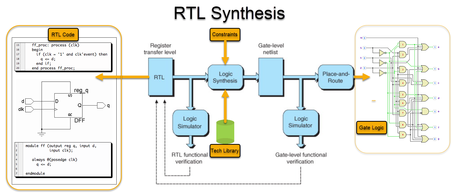
Synthesis: A powerful software tool called a synthesis tool takes our Verilog RTL code as input and automatically converts it into a list of digital logic gates (like AND, OR, NOT, and flip-flops). The output is called a netlist.
Physical Design (Place & Route): This stage is like creating the layout for a city. The synthesis tool's netlist is used to physically place the millions of gates onto the silicon die and then meticulously route the tiny metal "wires" to connect them all.
Tape-out: This is the final step where the design is sent to a fabrication plant (a "fab") to be manufactured.
🧠 Interview Focus: When an interviewer asks, "Can you walk me through the VLSI design flow?" you should be able to list these stages and briefly explain what happens in each one. This shows you understand the entire ecosystem, not just the coding part.
The Role of Verilog in the VLSI Flow
This is the most critical part for setting the stage for a learning Verilog :
Modeling (Behavioral/RTL): Verilog is first used to write the Register Transfer Level (RTL) description—the structural and functional design of the chip. This code describes how data moves between registers and how combinational logic processes it.
Simulation (Verification): Verilog code is fed into a simulator (e.g., Questa, VCS etc) to check if the design works correctly before it becomes physical hardware.
Synthesis: The Verilog RTL code is processed by a Synthesis Tool (e.g., Synopsys Design Compiler). This tool translates the HDL into an optimized gate-level netlist (a blueprint of actual logic gates: AND, OR, Flip-Flops) based on a target technology library. This translation is the bridge between code and physical chip.

